

Take Advantage of the ?Silent Switcher? Architecture
- January 26 2018
- Commercial Announcement
- 2619 Reads
- 0 Comments
How Does It Work?
The first generation of ?Silent Switcher? architecture used in IC LT8614, LT8640, and LT8641 reduces EM emissions by:
1. IC internal structure design and optimally placed package pins
2. well-controlled rising and falling edges
3. correct printed circuit board (PCB) design, which minimizes area of ?hot loops? on PCB
4. minimization of GND impedance on PCBS
5. switching frequency spread spectrum modulation
Enhanced ?Silent Switcher 2? version implemented in IC LT8609S, LT8640S, LT8643S, LT8645S goes even further:
1. IC contains internal ground plane and the use of copper pillars instead of bond wires
2. IC integrates capacitors connected to pins BST and INTVcc, further minimizing the "hot loop"
How Are Rising/Falling Edges Associated With The Signal Spectrum?
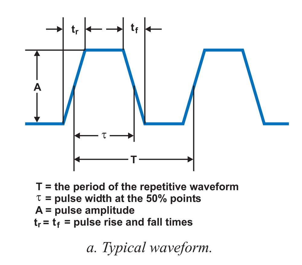
Another source of high frequency (hf) energy is ringing on edges. Waveform can look like this:
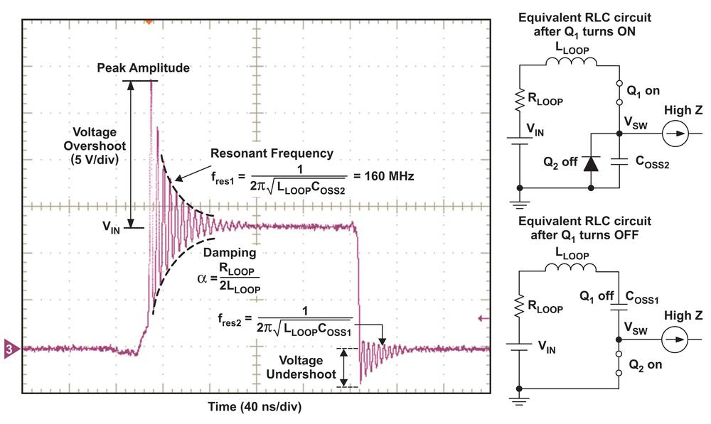
but also like this:

Rise and fall time is in range of ns, yet the first circuit of this series, LT8614, has switching edges almost without ringing. The steeper the switching edges, the more the high frequency components signal contains. The higher frequency, the shorter antenna is required for the effective emissions. We don?t add antenna to circuit intentionally but many structures used as a part of system or PCB are antennas.
Radiation from Switching Voltage Regulator
Radiation can occur as either differential mode or common mode.
Differential-mode radiation is the result of the normal operation of the circuit and results from current flowing around loops formed by the conductors of the circuit. These loops act as small loop antennas that radiate predominately magnetic fields. Although these signal loops are necessary for circuit operation, their size and area must be controlled during the design process to minimize the radiation.
Common-mode radiation is the result of parasitics in the circuit and results from voltage drops in the conductors. The current that flows through the ground impedance produces a voltage drop. When cables are then connected to the system, they are driven by this common-mode ground potential, forming antennas, which radiate predominately electric fields. Because these parasitic impedances are not intentionally added to the system or mentioned in the documentation, common-mode radiation is often harder to understand and control.
Why Minimize Area of the?Hot Loops??
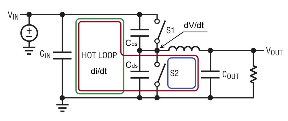
When S1 is ON (after turning off S1 and turning on S2), current flows in red (blue) and green loop. di/dt in red and blue loop is limited by coil inductance. Current waveform is DC with superimposed triangle waveform. di/dt in green loop is limited only by parasitics and it is far greater than di/dt in red or blue loop. The green loop is our ?hot loop?. Cds on the picture below is parasitic capacitance between mosfet S1 or S2 drain and source.
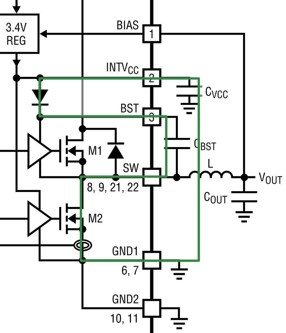
Another ?hot loop? is the boost circuitry.
Current flowing in the ?hot loop? creates loop antenna. For loop perimeter lower than ? of wavelength, maximal intensity of electric field occurs parallel to loop.
E=K1 f2 A I_dm
? f ? switching frequency and their harmonics
? I_dm ? current flowing in the loop
? A ? loop area
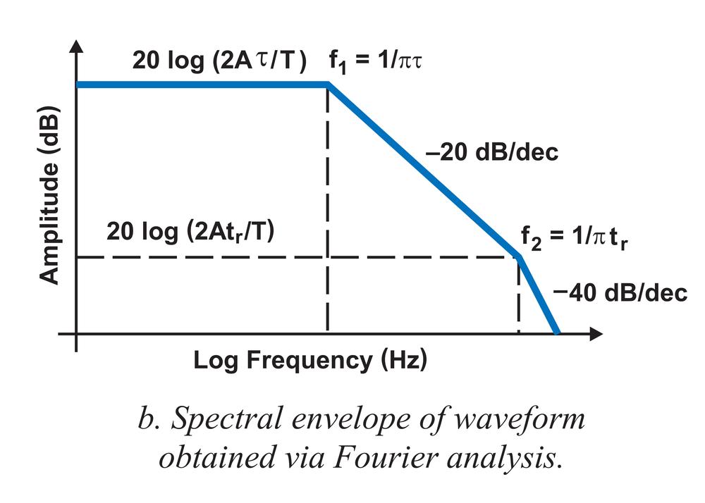
When we combine spectrum envelope of trapezoidal signal with frequency characteristics of loop antenna (f2 -> 20 log f2 = 40 log f => 40db/dec) we obtain differential-mode radiation emissions envelope.
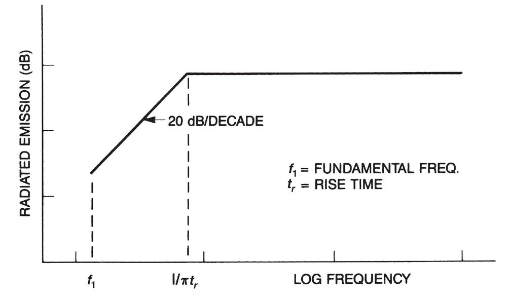
Envelope holds true for the frequency range where loop perimeter is smaller than ? of wavelength.
Example: Wavelength for frequency 1Ghz (upper limit for measuring radiated emissions during EMC tests) is Lambda=c/f=3e8/1e9=0,3m =>Lambda/4=75mm. Loop perimeter on PCB is typically smaller than 75mm, differential-mode radiation emissions envelope holds true for such a loop.
Steep switching edges are required for normal operation of IC; the only way how to minimize radiation is minimizing the loop area by correct design of PCB.
Why Minimize GND Impedance?
Currents flowing through GND impedance create voltage drops. When frequency rises, impedance also rises due to inductance of GND tracks. When antenna is connected to GND, problem with EMC arises. Such antennas can be modeled as short dipole.
Intensity of electrical field E = K2 f L I_cm
? f ? switching frequency and their harmonics
? I_cm ? antenna current
? L ? antenna length
When we combine spectrum envelope of trapezoidal signal with the frequency characteristic of antenna, we obtain common-mode radiation emissions envelope.
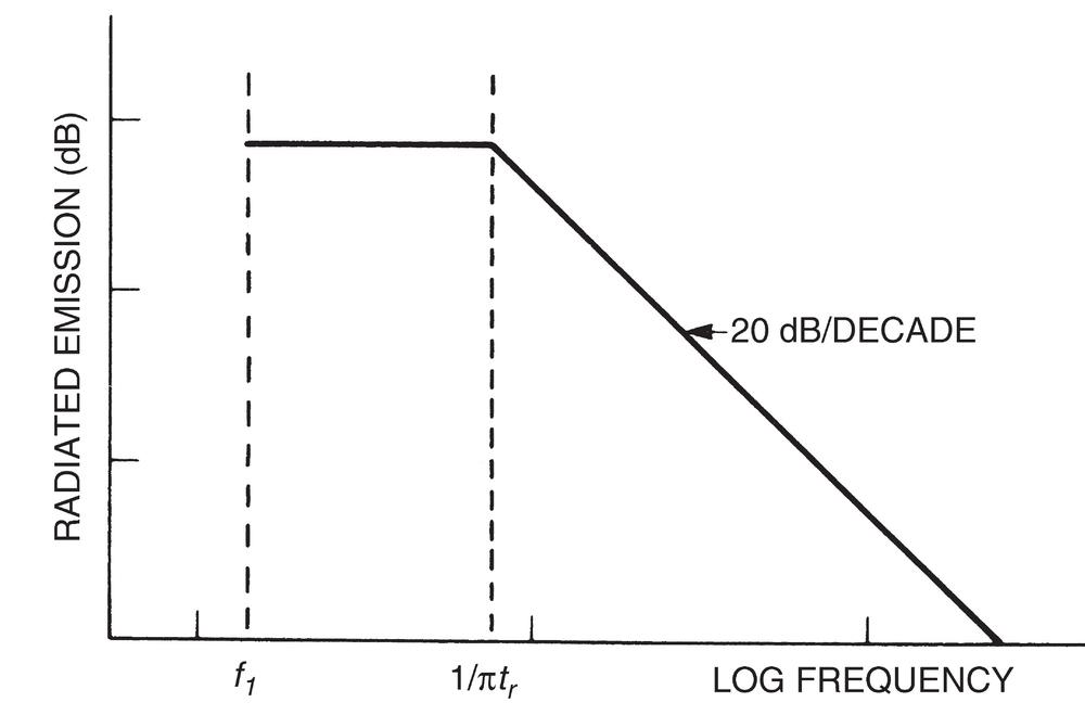
When we compare envelopes for common-mode and differential-mode, it might seem that common- mode emission is more likely to be a problem at low frequencies, while differential-mode emission is more likely to be a problem at high frequencies.
If the electric field intensity created by differential-mode emission is the same as for common mode, then K1 f2 A I_dm = K2 f L I_cm. By solving I_dm/I_cm we get
I_dm/I_cm=K2 L/ K1 f A = 48e6 L/f A [Henry W. Ott, Electromagnetic Engineering Compatibility]
pre f=100MHz, loop perimeter 40mm => A=127,3mm2=127,3e-6m2, and cable (antenna) length 1m je I_dm/I_cm= 3770
In other words, the common-mode radiation mechanism is far more efficient than the differential-mode radiation mechanism.
To minimize common-mode radiation, we have to minimize GND impedance.
How Spread Spectrum Helps?
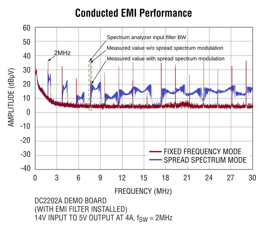
Power supplies generally fail EMC tests, not because of excessive total spectral energy but because of concentrated energy in a narrow frequency band around switching frequency harmonics. Frequency modulation of switching frequency doesn?t change the total amount of energy but spreads the energy to frequency band wider than input bandwidth of spectrum analyzer used during EMC tests. ?Silent Switcher? architecture modulates switching frequency in a range around 20% by using the triangle waveform signal.
For more info about products of Linear Technology, contact us on info@soselectronic.com
Features:
Ultralow EM Emissions
Spread Spectrum Frequency Modulation
Efficiency up to 95% at 1MHz, Up to 94% at 2MHz
Wide Input Voltage Range: 3V to 65V (LT8641, LT8645S), 3,4 to 42V (LT8614, LT8640, LT8609S, LT8640S, LT8643S)
Output currents: LT 8609S 2A, LT8641 3,5A LT8614 4A, LT8640 5A, LT8640S and LT8643S 6A, LT8645S 8A
Designed to comply with AEC-Q100: LT8609S, LT8641, LT8640, LT7640S, LT8645S
Source: https://www.soselectronic.com/