

Welcome to the 3D FLASH Memory World
- April 15 2018
- Commercial Announcement
- 2101 Reads
- 0 Comments
Apacer will use Toshiba chips manufactured by BiCS3 TLC NAND process, which guarantees 3 000 P/E cycles. 3D NAND TLC products will be covered by the same warranty as 2D NAND MLC based products; i.e. 2 years or the period ending on the date when the SSD has exceeded 3 000Average Erase Count, which is indicated by Apacer?s SMART software.
2D FLASH Technology Reaches Manufacturing Limits
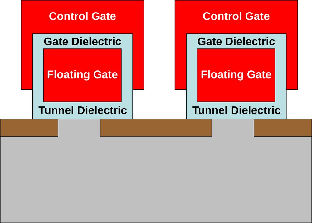
Current generation of Apacer SSD is based on 2D MLC flash memories produced by 15nm process. Low number of electrons that can be stored in the floating gate (FG) and the increasing interference between adjacent memory cells keep the chip capacity from increasing by reducing the geometry of the manufacturing process . With the reduction of the memory cell size, the floating gate (FG) is also reduced in the x-axis direction.
With unchanged gate thickness, the number of electrons that can be stored in the gate decreases, so the thickness of the gate must therefore be increased. However, as the cells get closer together, the capacity between the FGs of the individual cells increases, thereby increasing their mutual influence.
To minimize the interference, the manufacturers modified the shape of the control gate (CG) to the "cap" around the FG. This way, the capacity between CG and FG was increased, while the capacity between adjacent FGs was decreased. A further decreasing ofdistance between cells is no longer possible because it would not leave space for the CG.
Will 2D NAND Disappear Soon from The Market?
Answer is NO.
3D NAND FLASH technology is cost effective compared to 2D MLC for SSD capacity 32GB and more. 2D NAND MLC and SLC based products will continue to be available for embedded devices requiring low cost (MLC) or maximum-reliable (SLC) data storage.
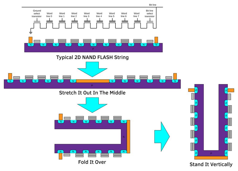
3D NAND FLASH
The principle of technology is explained in the following figure.
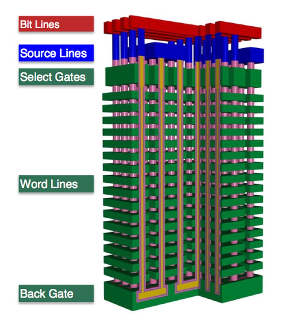
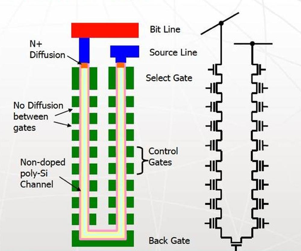
A closer look as BiCS NAND FLASH looks like is in the following figure.
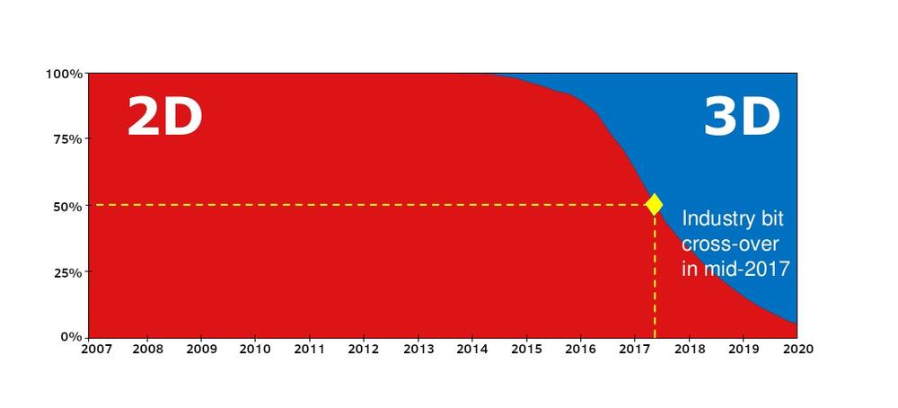
The 3D NAND manufacturing technology is mature nowadays. Since mid-2017, approximately 50% of FLASH chips have been manufactured using 3D NAND technology.
3D NAND FLASH Features
Larger memory capacity on the same chip area
15nm 2D MLC FLASH technology allows 128Gb/chip, BiCS3 3D TLC NAND allows 512Gb/chip.
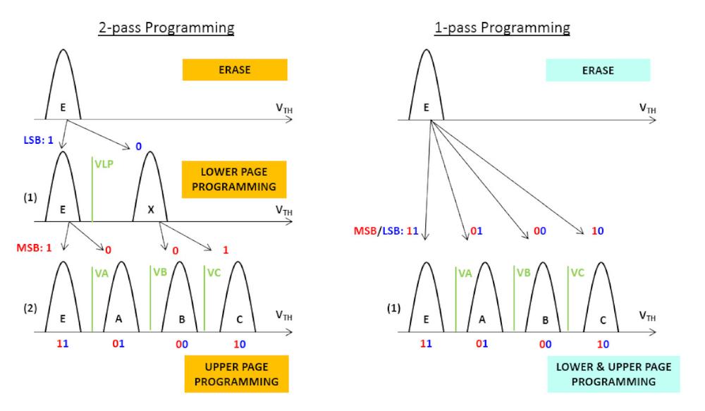
Faster programming, higher reliability, lower power consumption
The gaps between the memory cells are wider, so the interference between adjacent cells are lowered. At the same time, it enables single-shot programming of MLC / TLC cells. 2D MLC cells are programmed in two steps. Removing one step reduces the error rate (BER) during programming. Single-shot programming simultaneously reduces power consumption.
We will keep you informed about new Apacer products that are based on 3D FLASH memories on our website. If you are interested, please do not hesitate to contact us at apacer@soselectronic.com